Diffusion-Wave Diagnostic Technologies
—————–
INTRODUCTION
—————–
Diffusion-Wave Diagnostic Technologies is a spin-off company from the Center for Advanced Diffusion-Wave and Photoacoustic Technologies (CADIPT) of the Mechanical and Industrial Engineering Department in the University of Toronto.
Diffusion-Wave Diagnostic Technologies is a company which has been developing a family of advanced metrology instruments and systems based on laser photo-thermal diagnostic techniques, such laser infrared radiometry (PTR) and (photo) pyroelectric devices for the semiconductor and integrated circuit manufacturing, metal processing, biomedical sensors and imaging applications.
Central to the technologies of Diffusion-Wave Diagnostic Technologies is the incorporation of novel, proprietary, highly efficient, waveforms into its instruments for improvement of signal-to-noise ratios and for signal baseline suppression with concomitant improvement of contrast.
—————–
What We Do:
—————–
Diffusion-Wave Diagnostic Technologies licenses, manufactures and sells advanced metrology imaging system for the global semiconductor industry, non-destructive testing imaging systems for automotive metal processing industry as well as non-contact and non-destructive sensors and imaging systems for biomedical applications.
Our patented and patent pending technologies are based on non-contact, non-intrusive laser photo-carrier radiometry (PCR) and Photo-thermal radiometry (PTR). Primary target market is non-destructive testing systems for automotive metal processing industry as well as semiconductor process control such as monitoring and inspecting ion implantation, ultra-shallow junctions, diffusion, surface electronic integrity inspection, and transport properties determination (carrier lifetime, diffusion coefficient, front surface recombination velocity…).
—————–
Uniqueness:
—————–
The superiority of our patented and patent pending, non-contact, non-destructive PTR and PCR technology is based on simpler signal generation and detection principle and a higher sensitivity of infrared (blackbody) emissions to free carrier plasma densities than existing solutions in the market. These characteristics result in better signal-to-noise ratios, higher resolution, faster speed, and better control of the effects of process contamination and/or damage. Our technology offers the ability to perform continuous in-situ monitoring of substrate or patterned wafers during any process step. Diffusion-Wave Diagnostic Technology is a natural fit for multifunction applications.
Products
Products and Support Program
Bio-Medical and Industrial Engineering Applications:
Dentistry:
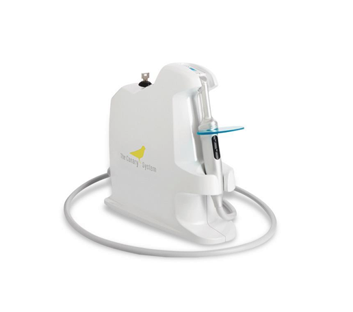
The Canary System
https://www.thecanarysystem.com
Diffusion Wave Diagnostic Technologies Online Tech and Training Support Program
For The Canary System: Contact email: info@diffusewavetech.com
Industrial Engineering Applications:
- License Photo-Carrier Diagnostics technology to Original Equipment (OEM’s) in order to introduce PCR technology in high volume fabrication plants.
- Stand alone, semi-automated tools instruments for the analog semiconductor industry (PCR-100).
- Low cost with limited automation instruments for the (R&D) labs.
Research
CASE STUDIES
—————–
CASE STUDIES 1: Carrier-Wave Radiometry:
—————–
Carrier-Wave Radiometry:
- Diffusion Wave Technologies currently holds two PTR patents in North America – two more (USA and PCT) pending – for its state-of-the-art photo-carrier radiometry (PCR) technology. PCR is the underlying fundamental technology behind our semiconductor metrology products. Diffusion Wave Technologies currently holds two PTR patents in North America – two more (USA and PCT) pending – for its state-of-the-art photo-carrier radiometry (PCR) technology. PCR is the underlying fundamental technology behind our semiconductor metrology products.
- The superiority of our patented, non-contact, non-destructive PCR technology is based on simpler signal generation and detection principle and a higher sensitivity of infrared (blackbody) emissions to free carrier plasma densities than existing solutions in the market.
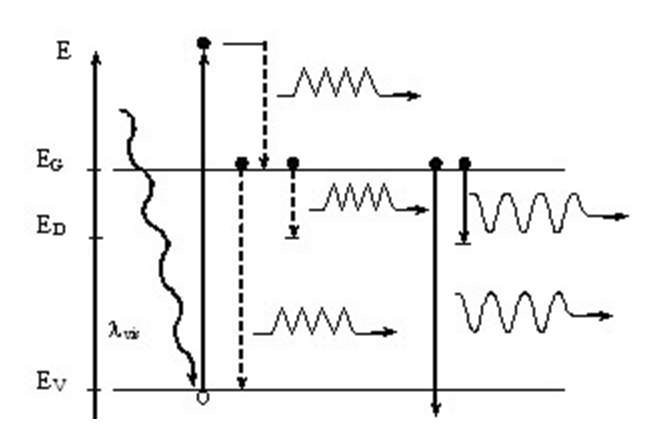
- n-type semiconductor energy-band diagram showing excitation and recombination processes. Energy emission processes include non-radiative intra band and inter band decay accompanied by phonon emission, as well as direct band-to-band recombination radiative emissions of energy and band-to-defect/impurity-state recombination IR emissions of energy.
—————–
CASE STUDIES 2: Photo-Carrier Radiometry (PCR):
—————–
Photo-Carrier Radiometry (PCR):
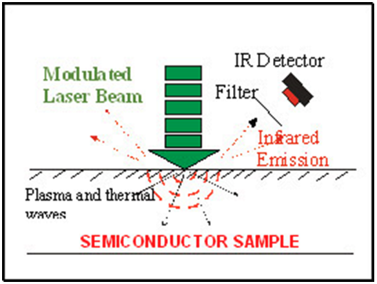
- Photo-thermal diagnostics are non-destructive testing methods complimentary to conventional methods such as ultrasound and X-ray inspection. Photo-thermal methods have advantages especially for near-surface (a few micrometers to a couple of millimeters) detection with a variable depth range, compared to conventional techniques. In this family of methods a beam of energy (typically a laser), intensity-modulated at a certain frequency, is focused onto the sample surface. The resulting periodic heat flow due to the absorbed optical energy in the material is a diffusive process, producing a periodic temperature distribution which is called a “thermal wave”.
- Photo-thermal applications include measurement of optical and thermal properties of a specimen as well as other aspects of the specimen which modify the temperature distribution such as thermal boundaries and defects in the sample. This requires the measurement of the periodic temperature at an external boundary of the specimen. There are several detection methods available to monitor the temperature. At CADIPT we use the IR radiometric detection method and in some cases where both thermal and optical measurements are required we use pyroelectric sensors (PVDF films). Pyroelectric-based photo-thermal devices and instruments for specialty analytical research projects are designed and built. The signal from the detector is sent to either (a) lock-in amplifier (b) box car integrator, or (c) FFT analyzer, depending on the measurement requirements. Other “conventional” photo-thermal instrumentation systems (spectroscopic, Mirage effect, photoacoustic) are also available.
Patents
—————–
1. “Non-contact photothermal method for measuring thermal diffusivity and electronic defect properties of solids”(Allowed September 1996. USA patent No. 5,667,300)
Inventors: Andreas Mandelis and Mahendra Munidasa.
2. “Non-contact photothermal method for measuring thermal diffusivity and electronic defect properties of solids”(Allowed in Canada March 27, 2001, patent No. 2,126,481)350
Inventors: Andreas Mandelis, Mahendra Munidasa, and D. wolf.
3. “Non-Contact Photothermal Methods for Measuring In-Situ Thermal Diffusivity of Solids”(Allowed September 16, 1997.
USA patent No. 5, 667, 300)
Inventors: Andreas Mandelis and Mahendra Munidasa.
4. “Non-contact photothermal radiometric metrologies and instrumentation for characterization of semiconductor wafers, devices and non electronic materials” (Full patent application submitted to Canada, April 17, 2000) Inventors: Andreas Mandelis, Jose A. Garcia, Lena Nicolaides, Mario Rodriguez, Stefano Pauloni.
5. “Method of Photo-Carrier Radiometry of semiconductors” Submitted to the USA and PCT patent offices, March, 2002 and 2003. Inventors: Andreas Mandelis, D. Shaugnessy, Jerias A. Batista, and Jose A. Garcia.
Publications
—————–
Diffusion Wave Technologies, in conjunction with CADIPT (https://cadipt.mie.utoronto.ca/publications/has produced the following Journal Publications and Conference Proceedings:
1. Infrared photocarrier radiometry of semiconductors: Physical principles, quantitative depth profilometry, and scanning imaging of deep subsurface electronic defects. A. Mandelis, J. Batista, and D. Shaughnessy. Physical Review B 67, 205208 (2003).
2. Temperature dependence of carrier mobility in Si wafers measured by infrared photocarrier radiometry. A. Mandelis, J. Batista, and D. Shaughnessy. Applied Physics Letter 82, 23 (2003).
3. M. E. Rodriguez, J. A. Garcia, A. Mandelis, C. Jean and Y. Riopel, “Kinetics of Surface-State Laser Annealing in Si Frequency-Swept Infrared Photothermal Radiometry”.Appl. Phys. Lett. 74, Number 17, 2429-2431, 26 April 1999.
4. T. Ikari, A. Salnick and A. Mandelis,”Theoretical and Experimental Aspects of Three-Dimensional Infrared Photothermal Radiometry of Semiconductors”.J. Appl. Phys. 85, Number 10, 7392-7397, 15 May 1999.
5. A. Salnick, A. Mandelis and C. Jean,”Infrared
Photothermal Radiometric Deep-Level Transient Spectroscopy of Shallow B+ Dopant States in p-Si”.
Appl. Phys. Lett. 71, No. 18, 2671-2673, November 1997.
6. A. Salnick, A. Mandelis and C. Jean, “Detection of Silicon Wafer Contamination by Lifetime Measurement Using Infrared Photothermal Radiometry”,
Phys. Stat. Solidi (a) Rapid Research Note 163, No. 1, R5-R6, September 1997.
7. A. Othonos, A. Salnick, A. Mandelis and C. Christofides, “Noncontact Carrier Lifetime Depth-Profiling of Ion-Implanted Si Using Photothermal Radiometry”.
Phys. Stat. Solidi (a) Rapid Research Note 161, R13-R14, 1997.
8. (Invited Review Paper) A. Mandelis, “Laser Infrared Photothermal Radiometry of Semiconductors: Principles and Applications to Solid-State Electronics”,
Solid-State Electron. 42, No. 1, 1-15, 1998.
9. (Invited) J. Shen, A. Mandelis and T.
Ashe,”Pyroelectric Thermal-Wave Resonant Cavity: A Precision Thermal Diffusivity Sensor for Gases and Vapors”,
Int. J. Thermophys. 19, No. 2, 579-593, 1998.
10. A. Salnick, A. Mandelis, H. Ruda and C. Jean, “Relative Sensitivity of Photomodulated Reflectance and Photothermal Infrared Radiometry to Thermal and Carrier Plasma Waves in Semiconductors”,
J. Appl. Phys. 82., No. 4, 1853-1859, August 1997.
11. A. Salnick, A. Mandelis, F. Funak and C. Jean, “Monitoring of ion Implantation in Si with Carrier Plasma Waves Using Infrared Photothermal Radiometry”,
Appl. Phys. Lett. 71, No. 11, 1531-1533, September 1997.
12. A. Salnick, C. Jean and A. Mandelis, “Noncontacting Photothermal Radiometry of SiO2/Si MOS Capacitor Structures”.
Solid State Electron 41 (4), 591-597 (1997).
13. A. Mandelis and R.E. Wagner, “Quantitative Photo-Thermo-Modulated Optical Reflectance Studies of Crystalline and Ion-Implanted Germanium”.
Jpn. J. Appl. Phys. 35 , 1786-1797, March 1996.
14. A. Salnick, A. Mandelis and C. Jean, “Non-Contact Measurement of Transport Properties of Long Bulk-Lifetime Si Wafers using Photothermal Radiometry”.
Appl. Phys. Lett. 69 (17), 2522-2524 , October 21, 1996.
15. A. Salnick, and A. Mandelis, “Hamiltonian Plasma-Harmonic Oscillator Theory: Generalized Depth Profilometry of Electronically Continuously Inhomogeneous Semiconductors and the Inverse Problem”.
J. Appl. Phys. 80 (9), 5278-5288 , November 1, 1996.
16. A. Othonos, C. Christofides and A. Mandelis, “Photothermal Radiometric Investigation of Implanted Silicon: The Influence of Dose and Thermal Annealing”.
Appl. Phys. Lett. 69 (6), 821-823, August 5, 1996.